Dive into the world of the Programmable Unijunction Transistor (PUT), exploring its structure, operation, applications, and advantages.

Introduction to Programmable Unijunction Transistor (PUT)
The Programmable Unijunction Transistor, commonly referred to as PUT, is a unique type of transistor. Unlike standard transistors that have three layers and two pn junctions, the PUT is a four-layer, three-junction device that exhibits a negative resistance characteristic. Its name, “programmable”, stems from the fact that the voltage at which it switches from high to low resistance (and vice versa) can be adjusted or “programmed” by altering the external components.
Structure and Principle of Operation
The structure of a PUT consists of four layers of alternating p and n type semiconductors. The layers are organized as p-n-p-n, similar to the structure of a thyristor. But unlike the thyristor, which has three terminals (anode, cathode, and gate), a PUT has only two: an anode and a cathode. The gate terminal of a PUT is derived from the n-type layer near the cathode.
The operation of a PUT is primarily based on the concept of a ‘breakdown voltage’. When the voltage applied to the device exceeds the breakdown voltage, the PUT switches from a state of high resistance (off-state) to a state of low resistance (on-state). This voltage, known as the peak point voltage, can be adjusted or ‘programmed’ by varying the ratio of two external resistors.
Applications of PUT
-
The PUT is commonly used in timing circuits due to its ability to switch states rapidly.
-
It is also utilized in oscillator circuits, where its negative resistance characteristic allows for the generation of oscillations.
-
In addition, PUTs are used in voltage and current regulator circuits due to their programmable switching voltage.
Advantages of PUT
-
The primary advantage of a PUT is its programmability, allowing for greater flexibility in circuit design.
-
It is a low-cost device, making it an economical choice for various applications.
-
PUTs are known for their reliability and long lifespan, making them a solid choice for circuits where stability is required.
The next part of the article will delve into the technical details of the PUT, including its symbol, characteristic curve, and the equation governing its peak point voltage.
Technical Details of PUT
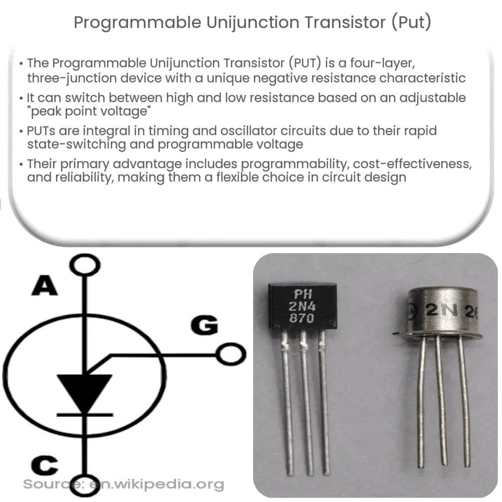
The PUT symbol resembles that of an NPN transistor but includes an additional line extending from the base to represent the gate. The anode is represented by the arrow, while the cathode and gate are denoted by the other two lines. When viewing the symbol, the anode is on the left, the cathode is on the right, and the gate protrudes from the cathode side.
Characteristic Curve
The characteristic curve of a PUT is a graphical representation of its current-voltage relationship. This curve has two distinct regions: the off-state and the on-state. In the off-state, the device exhibits high resistance, and the current through it is minimal. As the voltage reaches the peak point voltage, the device switches to the on-state, where it exhibits low resistance and allows a larger current to flow. This transition gives the curve its unique “N” shape.
Peak Point Voltage
The peak point voltage, denoted by VP, is the voltage at which the PUT switches from the off-state to the on-state. This can be calculated using the formula:
VP = VBB * (R2 / (R1 + R2)) + VI
Where VBB is the supply voltage, R1 and R2 are the external resistors, and VI is the intrinsic stand-off ratio.
Conclusion
The Programmable Unijunction Transistor (PUT) is a versatile and economical device that finds numerous applications in electronic circuit design, particularly in timing and oscillator circuits. Its unique structure, adjustable peak point voltage, and negative resistance characteristic distinguish it from other types of transistors. Understanding its working principle and the ability to control its switching voltage make the PUT a powerful tool for electronics engineers and hobbyists alike.


